You are currently viewing only those items made visible to the public. Sign in here with your UCL username and password to view the full catalogue.
Browse Items
Viewing items matching the following properties:
-
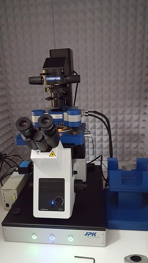
JPK Nanowizard Ultra Speed
The LCN is equipped with a JPK Nanowizard Ultra Speed AFM for fast scanning at up to 300Hz line rate in air and liquid at high resolution. It comes equipped with QI mode for quantitative material property mapping and the ability to correlate optical
more details » -
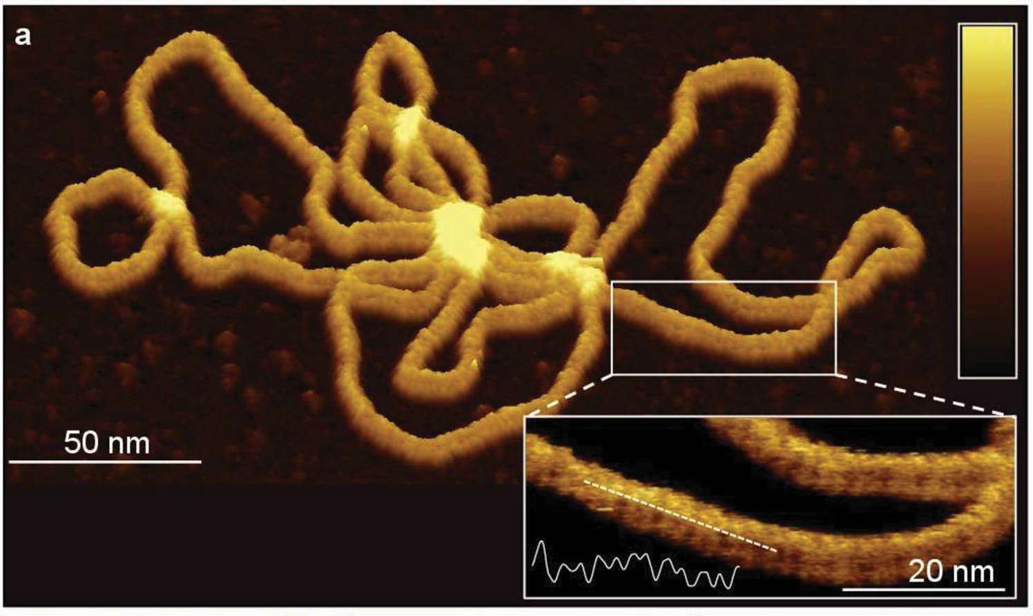
LCN Atomic Force Microscopy
The London Centre for Nanotechnology (LCN) offers an extensive suite of atomic force microscopes for nano-scale surface characterisation and functional imaging under ambient conditions (gas/liquid), including a Bruker Multimode, a Bruker Dimension 31
more details » -
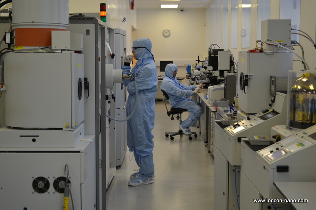
LCN Cleanroom Facility
The LCN Bloomsbury site has 255 m2 of Class 1000 (ISO 6) cleanroom housing the majority of the equipment including Electron Beam Lithography and an ISO7 facility which houses two Focused Ion Beam (FIB) lithography tools. There is also a Back End Lab
more details » -

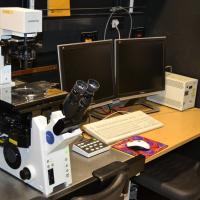
LCN Confocal and fluorescent microscopy
Confocal and Fluorescent Microscopy facilities at LCN.
more details » -
-
-
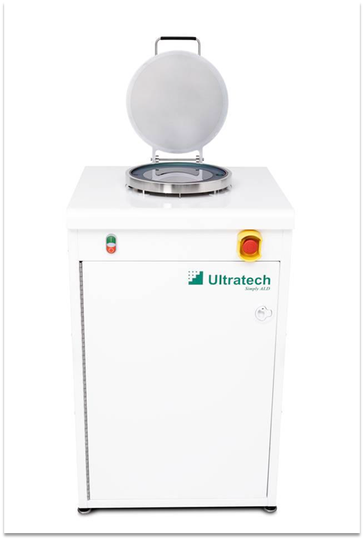
Atomic Layer Deposition (ALD) Equipment
We have a Savannah S200 ALD system, equipped with 6 precursor ports, a fomblin vacuum pump, Ozone generator and a Quartz Crystal Monitor.
more details » -
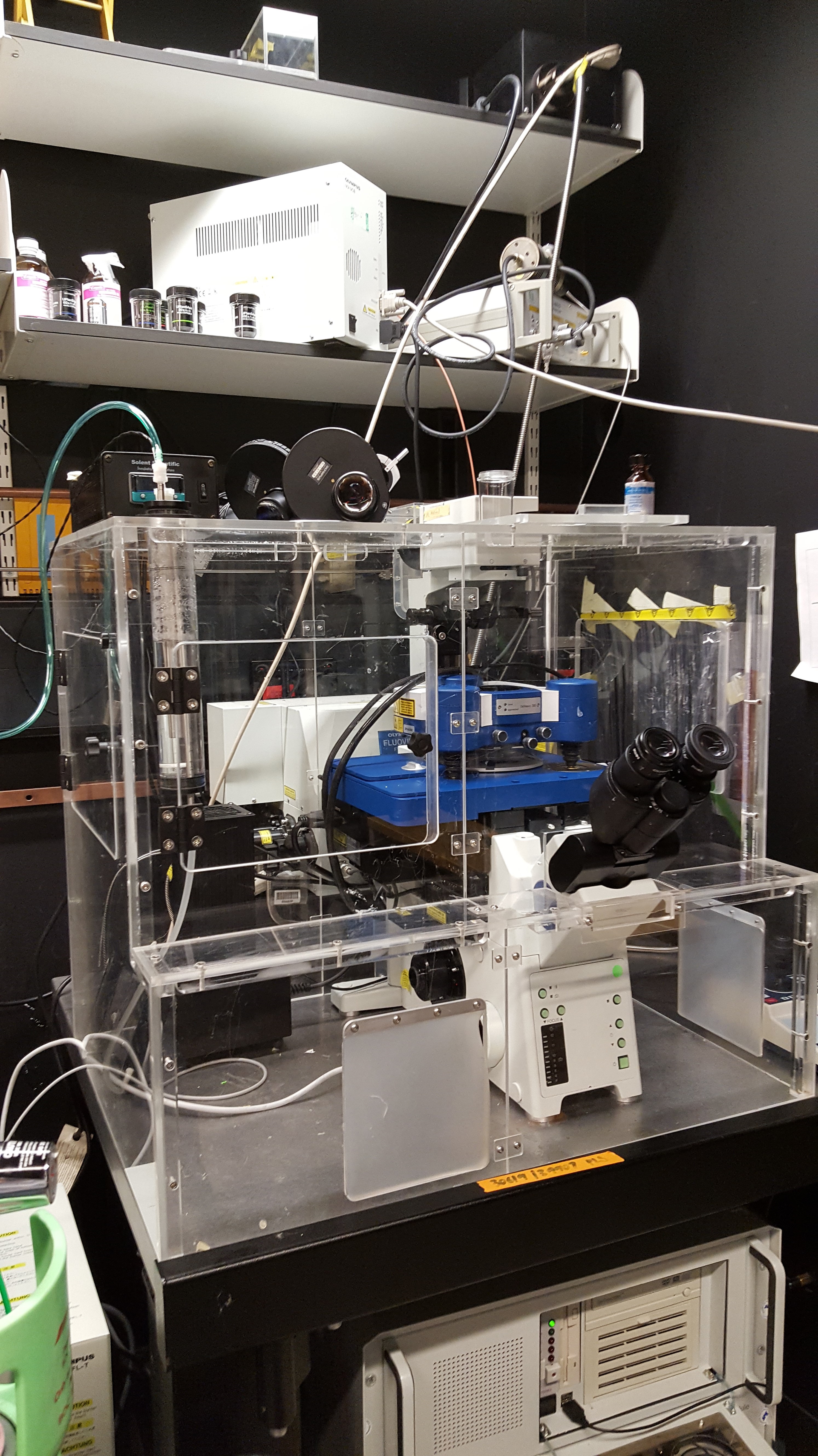
CellHesion 200 - measurement of cell adhesion & elasticity
Quantitative measurements of cellular adhesion and cell elasticity
more details » -

Closed cycle dilution refrigerator, with load-lock and magnet
<10 mK base temperature, 3/1/1T vector magnet, fast sample exchange
more details » -
-
-
-
-

Dilution refrigerator, superconducting and high permeability shielding, multi rf, dc wiring and filtering
Dilution fridge with rf and dc wiring connections
more details » -
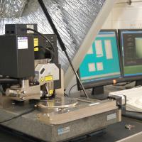
Dimension 3100 AFM
The Dimension 3100 utilises standard and advanced SPM imaging modes for measuring semiconductor wafers, lithography masks, magnetic media, biomaterials, optics and other materials
more details » -
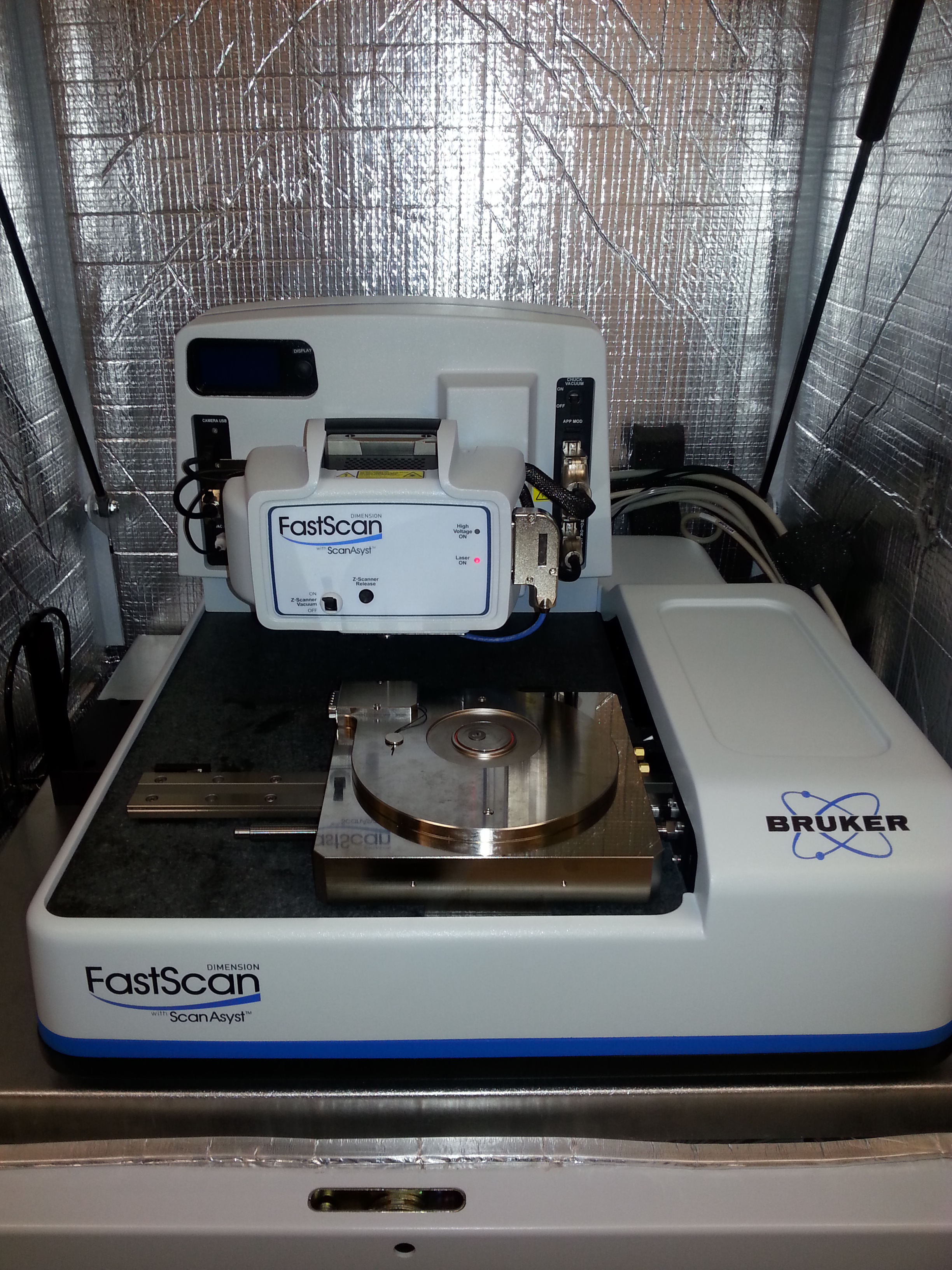
Dimension FastScan
The Dimension FastScan uses a low noise FastScan scanner and utilises PeakForce Tapping™ technology to provide new information, faster results and greatly improved ease of use in air or liquid.
more details » -
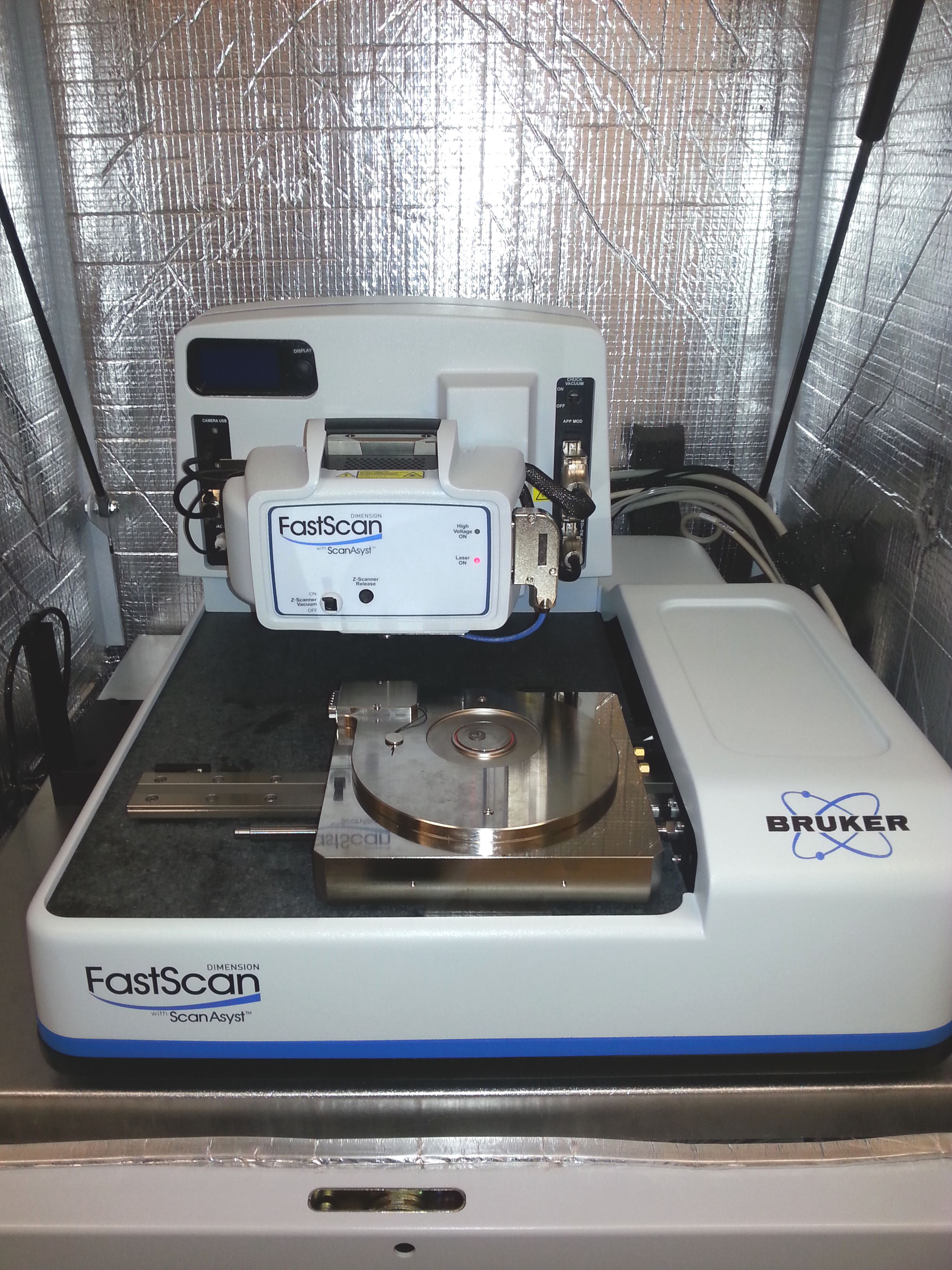
Dimension Icon
The Dimension Icon utilises PeakForce Tapping™ technology to provide new information, faster results and greatly improved ease of use in air or liquid.
more details » -
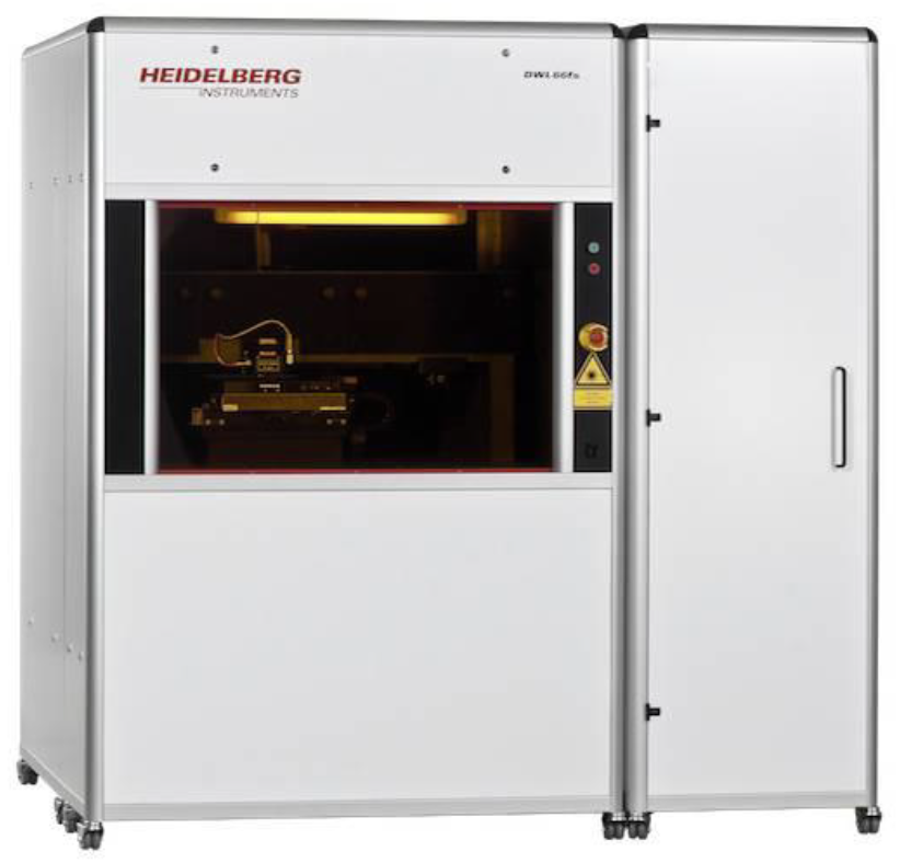
Direct Write Laser Lithography
A system for performing Photolithography without need for Photomasks
more details » -
-
-
-
-
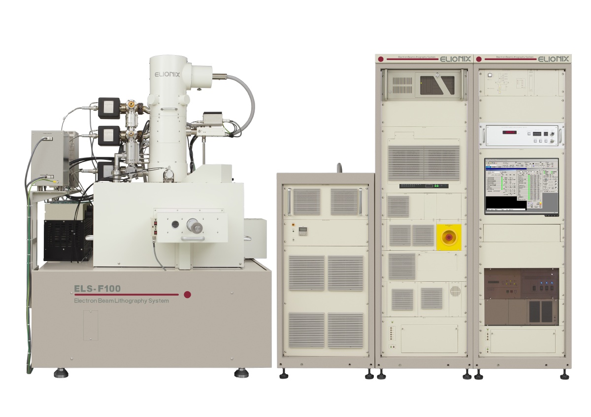
Electron Beam Lithography 100kV
Electron Beam Lithography
more details » -
-
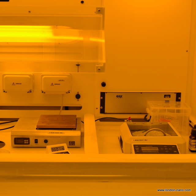
Electron Beam Resist Spin Coating & Baking
Spin Coater and Hotplate dedicated for Electron Beam Resist
more details » -
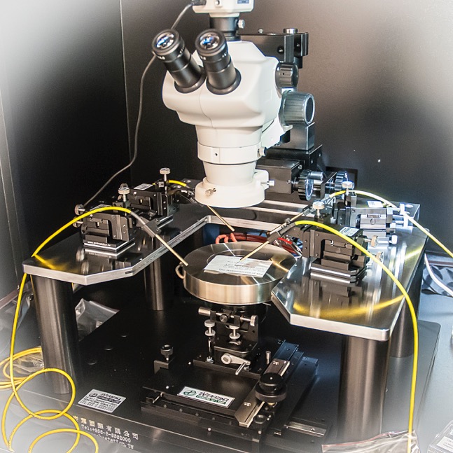
Everbeing EB-6 DC Probe Station
High precision probe station for DC wafer probing.
more details » -
-
-
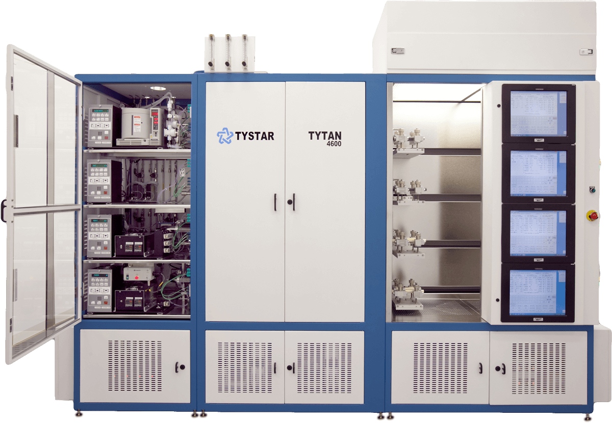
Furnace Stack
A system containing four independent Furnace tubes for Silicon wafers up to 150mm diameter
more details » -
-
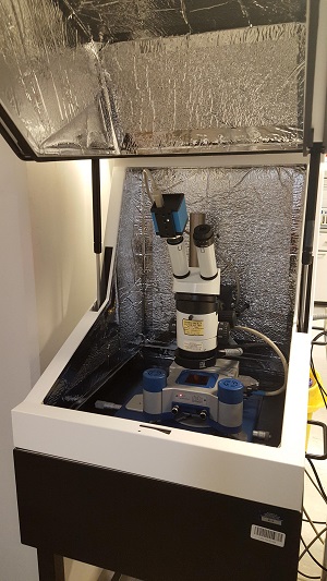
JPK Nanowizard 1 AFM with upright optics
The JPK Nanowizard Atomic Force Microscopes provide high resolution imaging of biological samples using a closed feedback loop to ensure precise positionining in the X,Y and Z dimensions.
more details » -
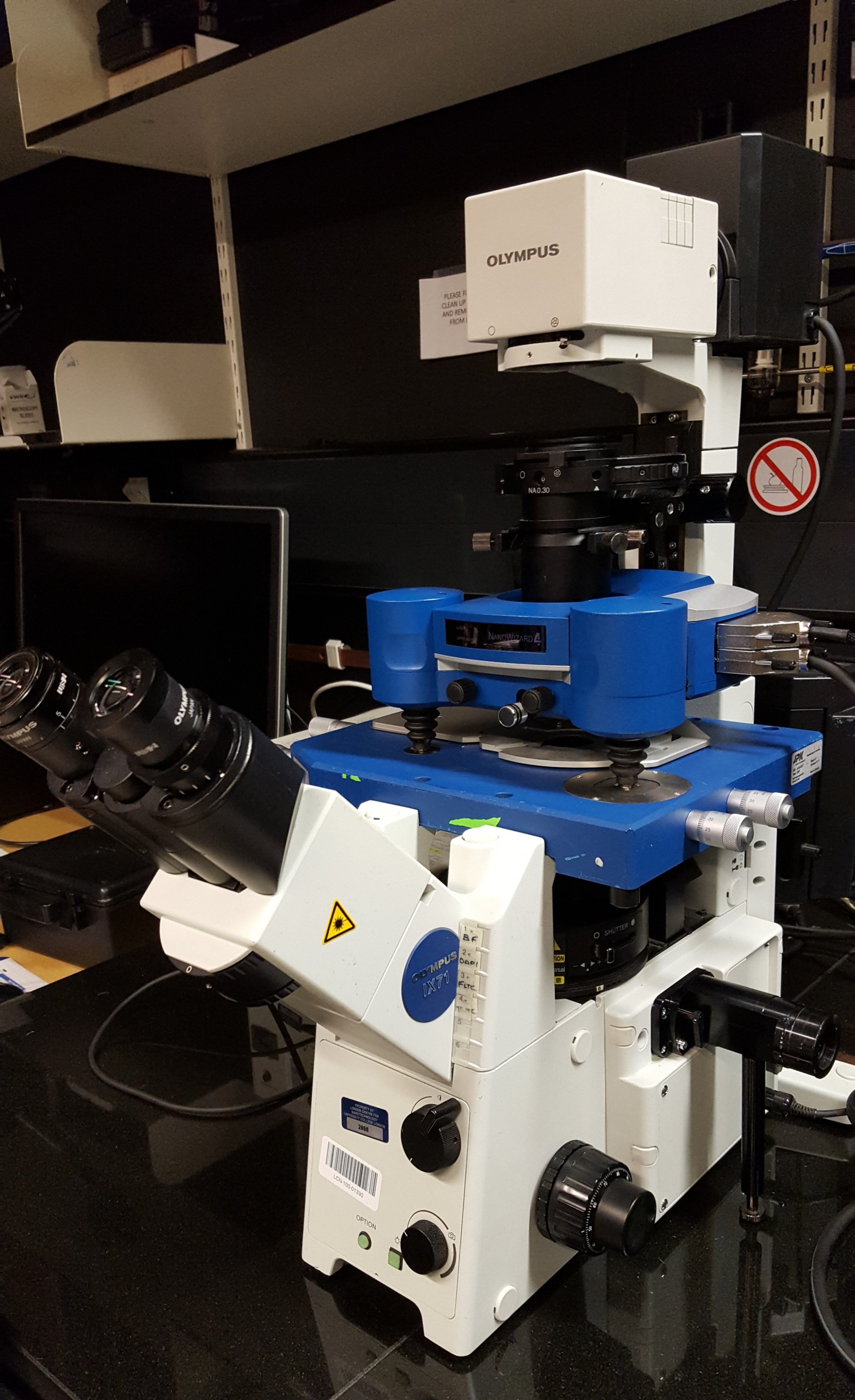
JPK Nanowizard 4 BioScience AFM
The JPK Nanowizard Atomic Force Microscopes provide high resolution imaging of biological samples using a closed feedback loop to ensure precise positionining in the X,Y and Z dimensions.
more details » -
-
-
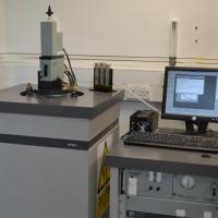
Magnetic Property Measurement System (MPMS-7)
The Magnetic Property Measurement System (MPMS) sample magnetometer utilises Superconducting Quantum Interference Device (SQUID) technology to achieve superior measurement sensitivity, dynamic range, and reproducibility otherwise unattainable.
more details » -
-
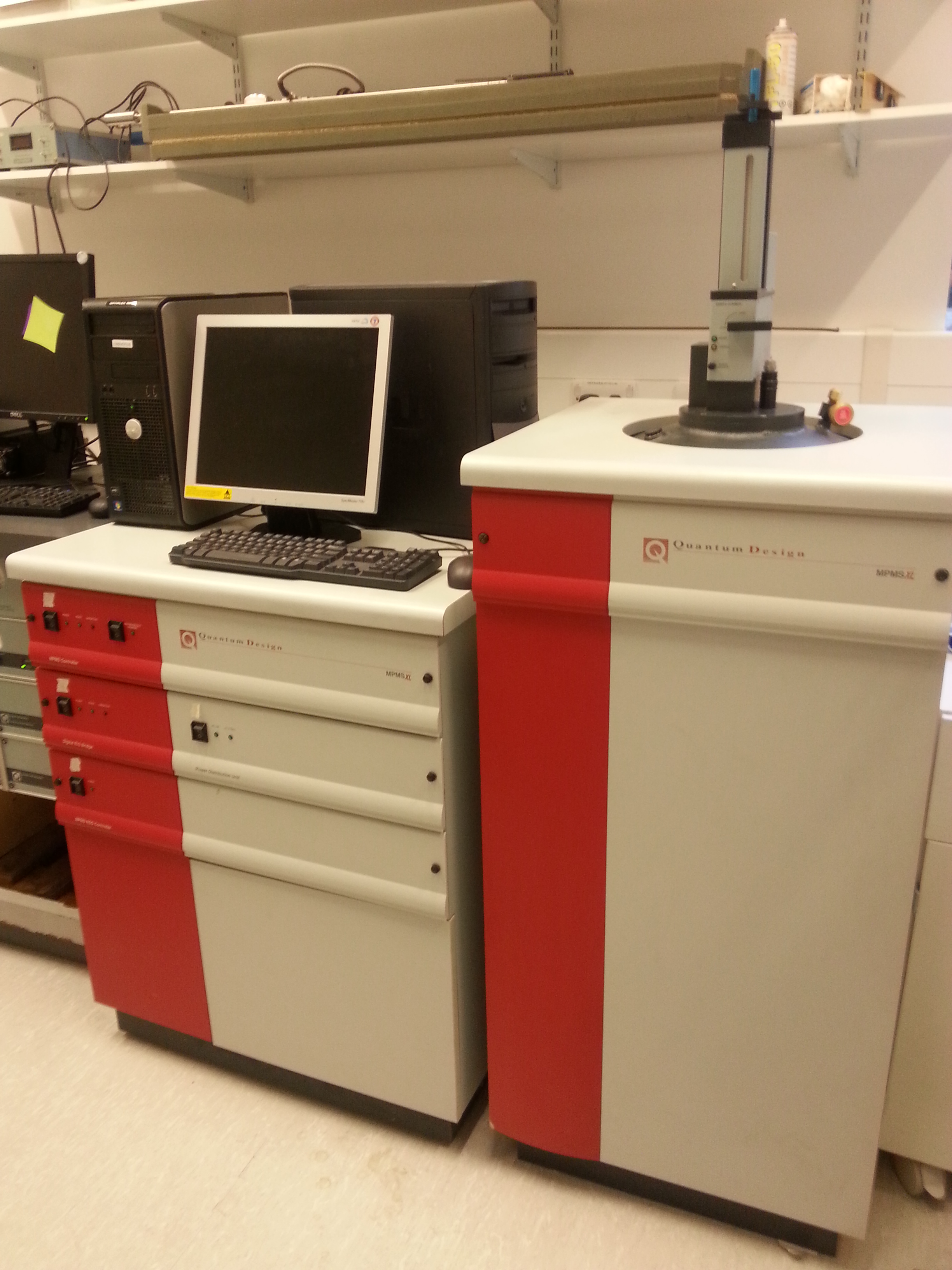
MPMS-XL
MPMS-XL for AC susceptibility measurements
more details » -
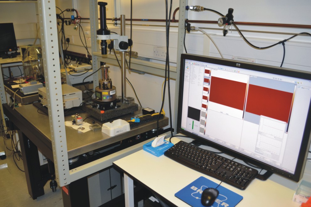
Multimode 8 AFM
The LCN has 3 Bruker MultiMode version 8 at the LCN each equipped with an E scanner or J scanner with heater and uses the unique PeakForce Tapping™ with ScanAsyst technology.
more details » -
-
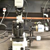
Olympus IX71 inverted phase/fluorescence microscopes
Fluorescence filter sets for 405, 488, 568, 647 nm excitation. Combined AFM capability with the JPK Nanowizard
more details » -
-
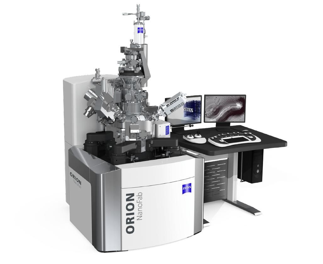
Orion NanoFab
Helium and Neon Scanning Ion Microscope for nanofabrication
more details » -
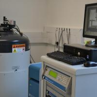
Physical Property Measurement System (PPMS)
The PPMS is an open architecture, variable temperature-field system, designed to perform a variety of automated measurements, with the following options: resistivity, AC-transport, heat capacity, ACMS, VSM and helium 3
more details » -
-
-
-
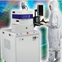
Reactive Ion Etcher
General Purpose Reactive Ion Etcher
more details » -
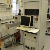
Shallow Reactive Ion Etcher
Chlorine and Fluorine chemistry Inductively Coupled Plasma RIE
more details » -
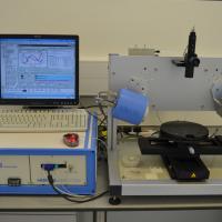
Spectroscopic Ellipsometer
For measurement of thin transparent films
more details » -
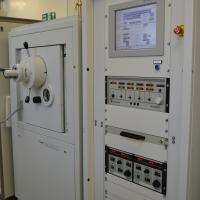
Sputter System
A four gun sputtering system plus Argon Ion Beam Milling capability
more details » -
-
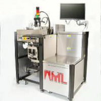
Wafer Bonder
A system that can perform bonding of two flat substrates. Techniques include anodic, adhesive and direct bonding
more details » -

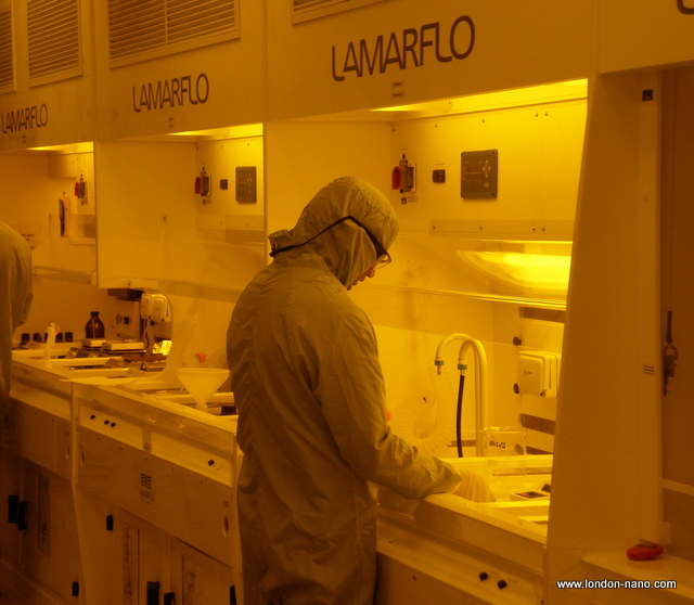
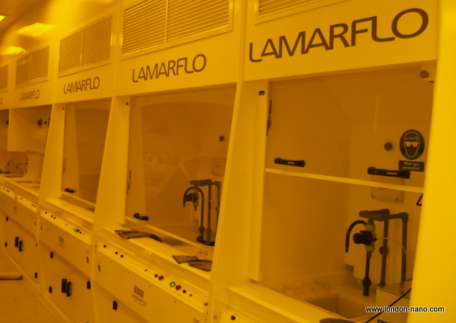
Wet Bench 2: Solvents
Dedicated to Solvent processes
more details » -
-
-
-
